THE DESIGN AND LAYERS OF PCB

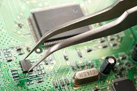
PCB (the Printing Circuit Board) are the building blocks of most electronics. It is a base that connects the electronic components. The PCBs are manufactured from fiberglass, composite epoxy, and other composite material. Copper traces, pads, stinks, planes are their conductive attributes. This mechanical structure is produced with insulating material covered between layers of conductive material. Overall, the PCB design is protected and plated with a nonconductive solder mask and silkscreen. The work of a PCB is to send signals to the electricity and brings the electronics to life.
These boards are usually connected to computers, and also associated with other electronic devices like TVs, radios, digital cameras, calculators, and cellphones.
APPLICATIONS
PCBs are also used in different fields other than in computers and consumer electronics.
- MEDICAL TOOLS: High-density PCBs with the smallest and densest designs are used in most medical instruments. For example, these are fixed in pacemakers, X-ray equipment, and CT scan machines.
- INDUSTRIAL MACHINERY: Current one-pounce PCBs and thick copper PCBs are used in high-powered industrial machines. The more abundant copper PCBs are beneficial for industrial load testers, high-current battery charges, and motor controllers.
- LIGHTING: The aluminum-backed PCBs high-lumen LED applications and basic lighting solutions. It grants a high level of heat transfer.
- AUTOMOTIVE AND AEROSPACE INDUSTRIES: The flexible PCBs used in the automotive and aerospace industries are fabricated to tolerate the high-vibration environment.
LAYERS
The several types of PCB boards have their own specific functions.
- SINGLE-LAYER PCBs: The single-layer PCBs are fixed in calculators, radios, cameras, and stereo instruments like printers, power supplies, and solid-state drives. This PCB is called a single-layer or single-sided PCB because it produced a single layer of substrate or base material. The one-side of the base material is laminated with a thin layer of metal, usually copper.
- DOUBLE-LAYER PCBs: A thin layer of conductive metal, like copper, is used as a base material in double-layer PCB, as it is applied to both sides of the board. One side of the circuits is connected to the other side through the drilled holes. These are used in LED lighting, Amplifiers, Vending machines, Automotive dashboards, HVAC systems, industrial controls, and power supplies.
- MULTI-LAYER PCB's: The PCB board design available in many layers such as thick multi-layer PCBs. They could be found in various sizes and layers. The 50-layer PCB was the biggest multi-layer PCB ever built. These PCBs are applicable in file servers, data storage, satellite systems, GPS technology, weather analysis, and other medical instruments.
